Clean Room Facility
The Clean Room lies at the heart of the research facilities at the Yousef Jameel Science and Technology Research Center. Inside the cleanroom are state-of-the-art facilities for developing MEMS/NEMS devices. This includes the Cryogenic Deep Reactive Ion Etcher (Cryo DRIE), capable of etching deep trenches with a high aspect ratio (up to 1:50). The Plasma Enhanced Chemical Vapor Deposition system (PECVD) is also available in the cleanroom for depositing low-stress thin films of various materials such as SiN, SiO2, SiC, doped, and undoped SiGe. Lithography facilities that include the EVG620 Mask Aligner, Spinner, and Wet Bench are also important parts of the cleanroom facilities. Other facilities include Tousimis Critical Point Drier, Wafer Geometry Gauge, and Surface Profiler.
For AUC internal user access requests, click here.
For Reservations:
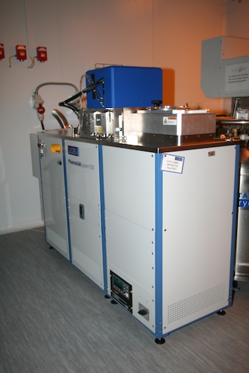
Model: OXFORD, PlasmalabSystem100 Modular Cluster System–ICP 65
A plasma etcher is a tool used in the production of semiconductor devices. A plasma etcher produces plasma from a process gas using a high-frequency electric field; a silicon wafer is placed in the plasma etcher, and the air is evacuated from the process chamber using a system of vacuum pumps. Then a process gas is introduced at low pressure and is excited into a plasma.
Specifications:
- 13.56 MHz driven parallel plate reactor
- kHz and "frequency mixing" optional
- Showerhead gas inlet optimized for
- Transfer station (square or hexagonal) vacuum cassette(s)
- Wide temperature range substrate electrode: -150° C - +400° C, RF driven
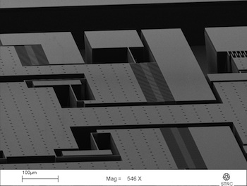
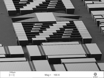
Plasma100 Chemical Vapor Deposition System from Oxford Instruments. The PECVD utilizes plasma technology to achieve high-quality thin-film depositions at temperatures up to 800 C.
The microfabrication group has developed several in-house recipes for SiGe, Poly-Si, SiC, SiN, and SiO2.
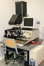
Lithography facility and the at the YJ-STRC include the Mask Aligner/UV Lithography EVG 620 and the Spinner for Lithography System LSM 200.
Mask Aligner/UV Lithography EVG 620
The EVG 620 Mask Aligner is a dual-use tool designed for optical double-side lithography and precision alignment up to 150 mm wafer sizes. The Mask Aligner is capable of transferring the designs of different MEMS/NEMS devices with high resolution.
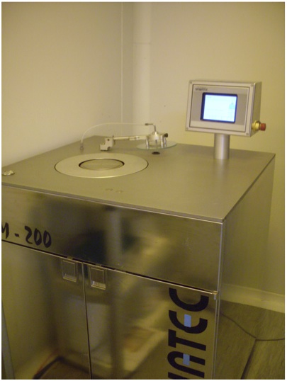
Spinner for Lithography System LSM200
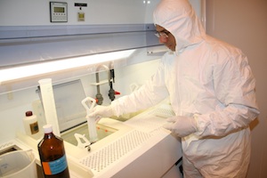
The Spinner from SawaTec, along with the Wet Bench, completes the set for the lithography. It is rotating stage equipment with optional RPM control used for the distribution of a coating substance on a wafer. It is used to coat the wafers with the PhotoResist material with controlled speed and acceleration. The Wet Bench is where the "wet processing" is carried out using different chemicals to resist development or wet etching.
Atomic Layer Deposition (ALD) is a thin film deposition technique that is based on the sequential use of a gas-phase chemical process.
Water purifier systems use successive steps of filtration and deionization to achieve a purity expediently characterized in terms of resistivity (typically 18.2 MΩ·cm at 25 °C). The system monitors the ion concentration by measuring the electrical resistivity of the water. Higher resistivity means fewer charge-carrying ions. Most Milli-Q systems dispense the water through a 0.22 μm membrane filter.

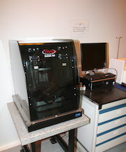
The Dektak Stylus Surface Profiler 150 uses a small tip to scan the surface of the wafers and provide a measurement of the features on top of the wafer. The measurements were taken to help to provide a view of the surface profile of the wafer to determine the etching depth on a wafer or the surface roughness, for example.
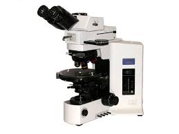
The optical microscope, often referred to as a light microscope, is a type of microscope that uses visible light and a system of lenses to magnify images of small samples.
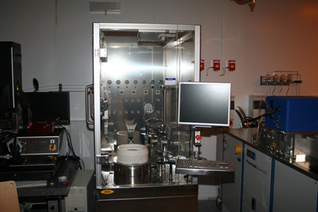
A coating is a covering that is applied to the surface of an object, usually referred to as the substrate. The purpose of applying the coating may be decorative, functional, or both. The coating itself may be an all-over coating, completely covering the substrate, or it may only cover parts of the substrate.
The MX 203-8-37 is a compact desktop instrument for the measurement of the geometry of silicon wafers. The gauge is based on two plates mounted opposite each other. Each plate contains a set of contactless capacitive sensors, they are arranged in a star-shaped pattern. On a kind of drawer, the wafer is manually inserted into the air gap between the two plates and then positioned on three resting pins for the measurement. The sensors measure the distances to the wafer surface; the results are sent to the connected PC via the serial interface.
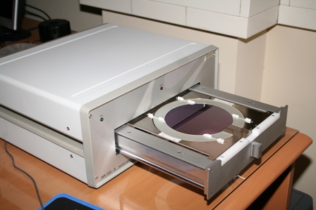
Based on these distance values, our supplied PC software computes the following wafer characteristics:
- Thickness related: Center-, Average-, Min.-, Max.- and Local Thickness, TTV
- Flatness related: Local FPD, max. Neg. FPD, max. Pos.FPD, TIR
- Warp related: Local Warp, Total Warp, Bow Local Stress, Average Stress, Center Stress
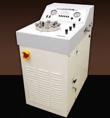
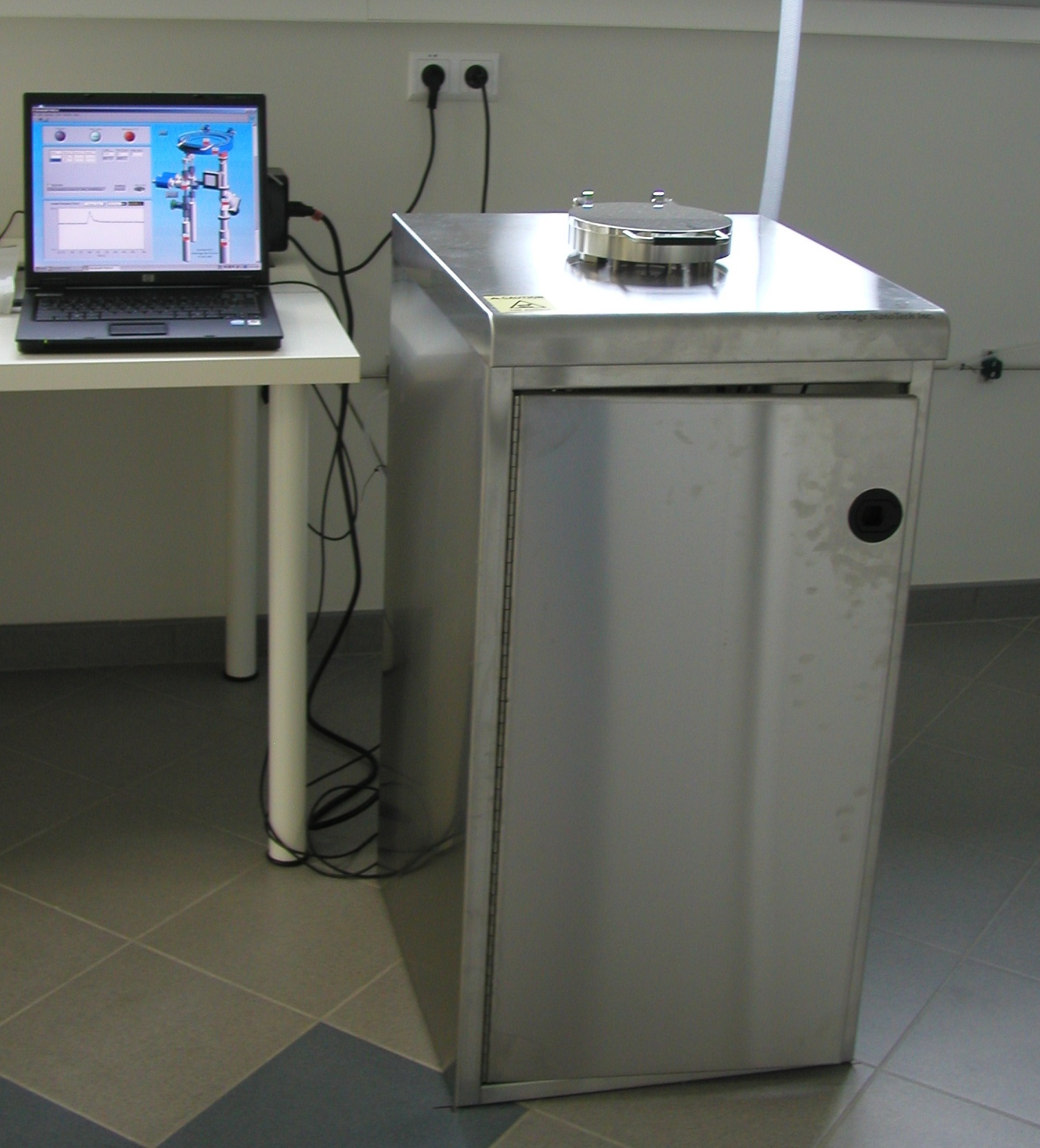
Critical Point Drying is so named as it includes, as part of its process, the occurrence known as the continuity of state for which there is no apparent difference between the liquid and gas state of a medium, the surface tension between this interface reducing to zero. This occurs at a specific temperature and pressure with resulting density and is known as the Critical Point. This condition of zero surface tension can be used to dry Biological Specimens, avoiding the damaging effects of surface tension.