Characterization Facility
- Centers and Labs
- Youssef Jameel Science and Technology
- Facilities
- Characterization Facility
Characterization refers to studying a material's features, such as its composition, structure, and various properties like physical, electrical, magnetic, and others.
For AUC internal user access requests, click here.
For SEM facilities, click here.
For Reservations:
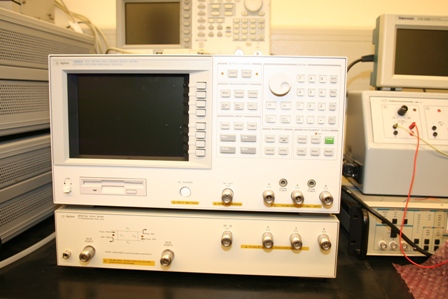
The HP Agilent 4395A provides an excellent RF vector network, spectrum, and optional impedance measurements for audio, baseband, HF, VHF, and IF applications. Gain, phase, group delay, distortion, spurious, CN ratio, and noise measurements are often required for evaluating components, and circuits can be measured using one instrument.
The Four-point Probe is an electrical impedance measuring technique that uses separate pairs of current-carrying and voltage-sensing electrodes to make more accurate measurements than the simpler and more usual two-terminal (2T) sensing. Four-terminal sensing is used in some ohmmeters and impedance analyzers and in wiring for strain gauges and resistance thermometers. Four-point probes are also used to measure the sheet resistance of thin films.
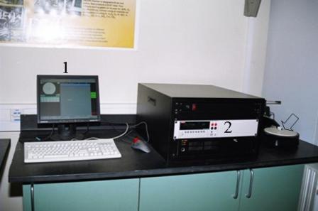
Computer-controlled four-point probe capable of measuring structures from 1mW/sq to 800 KW/sq, with an accuracy better than 1%.
- Resistivity control software with output: 2D Contour Map/3D contour map/diameter plot
- Programmable current source and digital multimeter
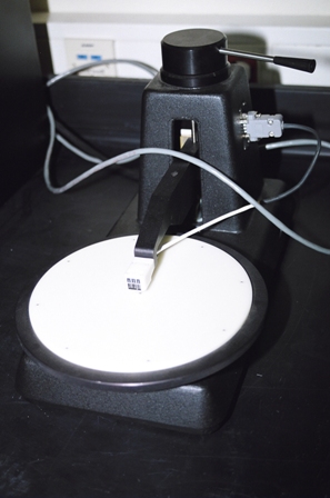
200 mm Teflon disk holds 10 mm to 200 mm samples.
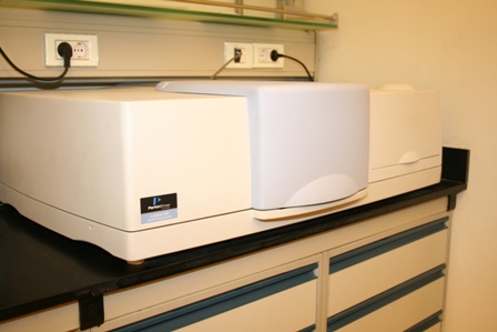
Spectrophotometry is the quantitative measurement of the reflection or transmission properties of a material as a function of wavelength. It deals with visible light, near-ultraviolet, and near-infrared.
The Agilent 4156C Precision Semiconductor Parameter Analyzer is a highly accurate laboratory benchtop solution for advanced device characterization. You can control your parameter analyzer from a PC with B1541A Desktop EasyEXPERT edit software that provides the same test and measurement environment for the B1500A Semiconductor Device Analyzer. The new version of Agilent Desktop EasyEXPERT software, which is included with the 4156C, is able to control the Agilent 4156C parameter analyzers too.
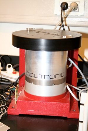
These single-axis rate tables are intended for use during development, production, in-process testing, calibration, and final inspection of inertial components, instruments, and MEMS sensors. The product was designed with an emphasis on easy use by customers and economic pricing.
Differential scanning calorimetry, or DSC, is a thermoanalytical technique in which the difference in the amount of heat required to increase the temperature of a sample and reference is measured as a function of temperature. Both the sample and reference are maintained at nearly the same temperature throughout the experiment.
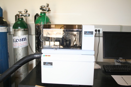
YJ-STRC has a Perkin Elmer power compensation DSC, ‘Diamond DSC’, that consists of two identical sample and reference furnaces equipped with precise Platinum resistance thermometers and two separate heaters built inside the furnaces. The device itself is equipped with both liquid nitrogen and mechanical cooling attachments, and an autosampler that facilitates handling of the sample and reference materials. The device operates by the simple concept of compensation of the power input to the furnaces in order to maintain the sample and reference temperature as closely as possible during a programmed temperature scan with a specified heating or cooling rate. The process takes place under nitrogen purge gas with a controlled flow rate. High-purity aluminum pans and covers are used to encapsulate the sample and reference materials using special crimping equipment.
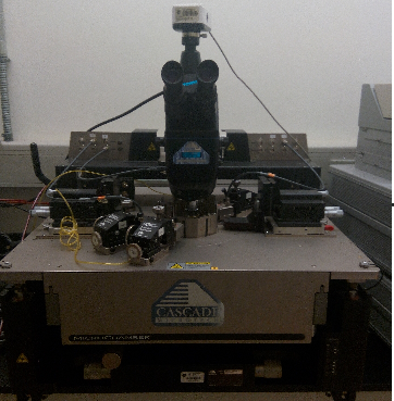
The SUMMIT series of semi-automated probe systems, with PureLine™ and AttoGuard® technologies, allow you to access the full range of your test instruments for wafers up to 200 mm. Whatever your application: RF/Microwave, device characterization, wafer-level reliability, e-test, modeling, or yield enhancement, the Summit leads the industry in on-wafer measurements. Summit series probe systems are easy to configure with your choice of measurement performance, chuck size, thermal range, and microscope options. All platforms are -60°C to 300°C compatible to ensure an upgrade path to meet your future needs. Cascade Microtech provides many accessories for the Summit for a wide range of applications to suit your unique wafer probing test needs.
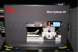
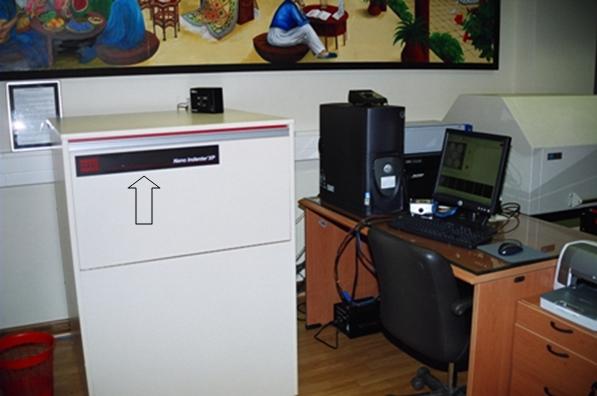
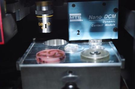
A nanoindenter is the main component for indentation hardness tests used in nanoindentation. Nanoindentation, also called depth-sensing indentation or instrumented indentation, gained popularity with the development of machines that could record small loads and displacements with high accuracy and precision. The load-displacement data can be used to determine the modulus of elasticity, hardness, yield strength, fracture toughness, scratch hardness, and wear properties. It has two modules: the DCM Module for thin films and the XP Module for Bulk Material.
In an AFM a constant force is maintained between the probe and sample while the probe is raster scanned across the surface. By monitoring the motion of the probe as it is scanned across the surface, a three-dimensional image of the surface is constructed. The Atomic Force microscope is a tool to study many properties on the nanometer and micrometer scale. Possible properties that can be studied: topography, roughness, magnetic properties, elastic properties, adhesion, etc. Furthermore, very small forces can be measured as well.
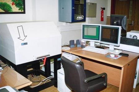
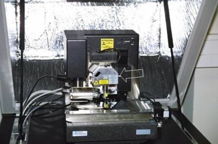
Model: VEECO Dimension 3100 Scanning Probe Microscope
The Dimension 3100 Scanning Probe Microscope (SPM) utilizes automated atomic force microscopy (AFM) and scanning tunneling microscopy (STM) techniques to measure surface characteristics for samples up to 200 mm in diameter. It performs all major AFM imaging techniques and modes.
Common Modes of Operation
Contact Mode
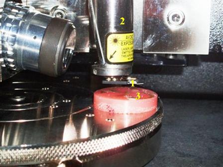
A sharp tip on the end of a flexible cantilever (1) is scanned by means of a piezoelectric tube scanner (2) across the sample surface (3) while maintaining a small constant force. The tip-sample interaction is monitored by reflecting a laser off the back of the cantilever into a split photodiode detector, which monitors the change in cantilever deflection. A feedback loop maintains a constant cantilever deflection. The vertical movement of the scanner forms the topographical image of the sample surface.
Tapping Mode
The cantilever is oscillated at its resonance frequency and taps the surface lightly during scanning. The changes in the tip oscillation amplitude are monitored. A feedback loop maintains a constant oscillation amplitude. The vertical movement of the scanner forms the topographical image of the sample surface. Tapping mode is used to image soft, fragile, and adhesive surfaces as it eliminates the lateral shear forces present in contact mode, which can damage such surfaces.
It is a spectroscopic technique used to observe vibrational, rotational, and other low-frequency modes in a system. Raman spectroscopy is commonly used in chemistry to provide a fingerprint by which molecules can be identified.
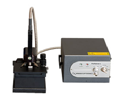
The optical profiler provides three-dimensional surface profile measurements without contact.
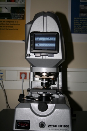
Model: VEECO WYKO NT1100
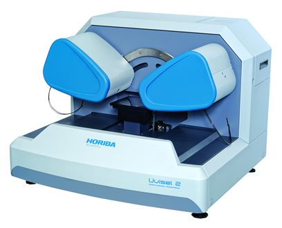
Ellipsometry measures a change in polarization as light reflects or transmits from a material structure. The polarization change is represented as an amplitude ratio, Ψ, and the phase difference, Δ. The measured response depends on the optical properties and thickness of individual materials. Thus, ellipsometry is primarily used to determine film thickness and optical constants. However, it is also applied to characterize composition, crystallinity, roughness, doping concentration, and other material properties associated with a change in optical response.
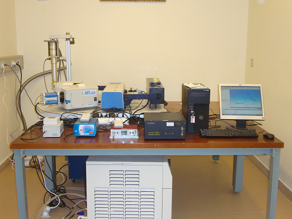
Photoluminescence spectroscopy is a non-contact, non-destructive method of probing the electronic structure of materials. In essence, light is directed onto a sample, where it is absorbed and where a process called photo-excitation can occur. The photo-excitation causes the material to jump to a higher electronic state and will then release energy (photons) as it relaxes and returns back to a lower energy level. The emission of light or luminescence through this process is photoluminescence, PL.
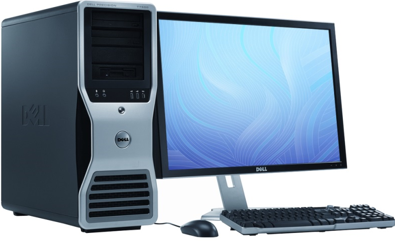
Workstation computer used for running simulation and analysis software.
