Samples of Prototypes
- Centers and Labs
- Center of Nanoelectronics and Devices
- CND Samples of Prototypes
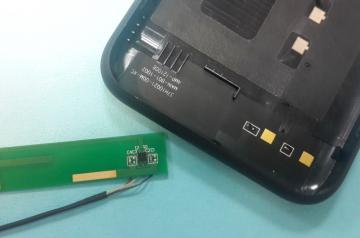
The tunable antenna for Reconfigurable IoT RF transceivers is a 2cm X 2cm square microstrip antenna designed with reconfigurable side length and corner dimensions. The side length tunes the antenna frequency, and the corner dimensions tune the antenna bandwidth. The reconfigurability is performed by using RF MEMS switches.
This chip is under fabrication in collaboration with the British University in Egypt (BUE), Cairo, and Bristol University, England, and with support from the ITIDA funding agency, Egypt.
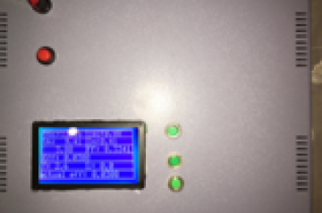
The center has built low budget solar characterizer to be used in conjunction with our solar panel models. The current direction is to use this as a nucleus for power generation SCADA systems and the industrial design to use it as a measurement device in the market.
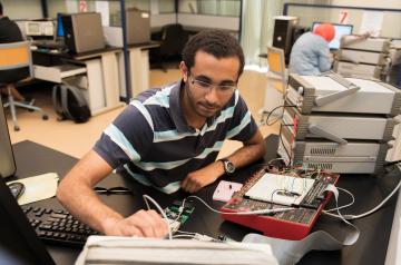
The center has developed a photovoltaic on-grid inverter for high-power applications. The cost of the system is very low compared to the industrially used systems. The inverter implements MPPT, is highly efficient, and is of easy to maintain and upgrade. The modality of the design makes the modification to support multiple power generation capacities very cheap. The prototype is now being industrially designed for market penetration.
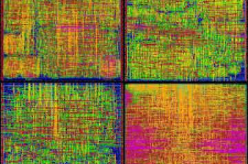
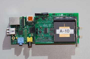
The low-power FPGA chip area is 3.2mm X 3.2mm in UMC 130nm CMOS technology. The chip is designed by implementing an embedded On-Chip Network (OCN) inside the FPGA chip to reduce the interconnect power and delay. This OCN is expected to increase the FPGA chip performance and reduce the routing complexity by providing a kind of highway inside the chip (OCN routers). The chip includes the FPGA fabric using 4-bit LUT, 3-LUTs cluster, 50% flexibility, and 24 bidirectional channels. It also includes 4 OCN routers with the required interface to talk to the fabric as well as the SRAM programmer required to configure the FPGA chip once fabricated. The chip is under fabrication with the support of FabCat (Fabrication Catalyst), Cairo, Egypt.
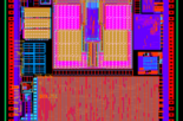
Chip Technology: UMC 130 nm
Area: 10.5 mm2
Description: This chip contains four innovative IPs that are implemented in fully QDI Asynchronous circuits. The designs target ultra-low-power applications such as wireless sensor nodes and IoT. Due to their asynchronous implementation, the designed IPs are very robust against the parameter changes, such as power supply levels, temperature, and process variability.
List of designed IPs:
- Optimized Asynchronous AES cryptoprocessor Asynchronous implementation for “PRESENT”. Lightweight encryption for IoT and WSN.
- Asynchronous implementation for “GRAIN”. An ultra-lightweight encryption for IoT and WSN.
- All Digital Test Pattern Generator Based on Self-Timed Rings.
Chip Technology: GF 65 nm (in collaboration with UAE)
Area: 12 mm2
Description: A body Sensor Network Chip that contains power management blocks, energy harvesting blocks, medical data analysis blocks, and asynchronous blocks.
DC-DC Converter: a hybrid converter for dynamic voltage scaling that is a mix between buck and switched capacitor converter. Measured results show an on-chip efficiency of 93% higher than anything reported in the literature.
ERUST: A new microarchitecture-level technique that is reducing power consumption. In this technique, we are using a modified razor architecture to make the circuit robust against error generation. When low power mode is activated, the supply voltage is reduced, and the critical path generates an error. The implemented architecture recovers the error by borrowing time slack from the successive pipeline stages. Measured results show that the pipeline can work correctly at the same frequency at a much lower supply voltage.
Energy Harvesting: including MPPT matching, self-starting blocks, mixer between light, thermal, and piezoelectric harvesters, and DC-DC converter.
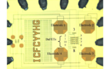
Chip Technology: CMOS 180nm TSMC technology
Area: 4 mm2
Objective: Leukemia Detection and Characterization
Description: The chip consists of two main parts. (1) The electric field generator part, which is a quadrupole electrode configuration to produce the required electric field profile. (2) the sensing part, which is an array of the Differential Electric Field Sensitive Field Effect Transistor (DeFET). Electric Field Generator Part: The used electrodes are the quadrupole configuration, see Figure 3 [5]. Using this configuration, we can control the profile of the electric field by connecting the whole four electrodes or some of them to the inputs that are received from the LabVIEW via the DAQ.
Sensing Part
The sensing part is composed of an array of DeFET sensors. We can detect the electric field by using the Electric Field Sensitive Field-Effect Transistor [eFET] as a novel electric field sensor. Figure 4 shows the schematic structure of the eFET. It consists of two adjacent drains, two adjacent floating gates with distance “Y” between them, and one source. For the eFET, it is equivalent to two identical enhancement MOSFET devices. Under the influence of the electric field, the current imbalances of the two drain currents occur. Due to the drain current dependence on the gate voltage, the eFET can sense the difference between the two gate voltage, which reflects the intensity of the applied electric field. To increase the measurement range of the eFET, we are using the CMOS concept to implement the Differential Electric Field Sensitive Field Effect Transistor (DeFET) sensor, and this sensor will be the basic sensing block in the sensing part of the proposed CMOS Biochip.
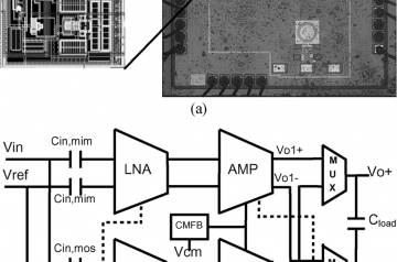
The neural interface chip area is 1.5mm X 1.5mm in 130 nm UMC CMOS technology. The chip is designed to be interfaced with deep brain stimulation electrodes of length 3mm with 256 monitoring channels (64 channels on 4 shafts) and 16 stimulation channels. The chip contains the required analog conditioning circuits such as 256 Low Noise Amplifiers (LNAs), 256 filters, 256X1 analog multiplexers, and 12-bit Time-Based Analog to Digital Converter (TADC). Moreover, it contains 16 stimulation channel for treatment that contains 8-bit Digital to Analog Converter (DAC), 1X 16 analog de-multiplexer, and 16 drivers. Following the analog conditioning circuits, there is a digital processing unit that is used to compress the data and make it read for transmission. The chip is under fabrication with the support of the ITIDA funding agency in Egypt and the collaboration with NOVELA incorporation, Waterloo, Ontario, Canada.
Eight Patents have been Granted since 2012 (some work done in the US)
- Infrared Subwavelength Focusing in Silicon and Energy Harvesting DevicesM Swillam, MA Abdel-Galil, Y Ismail, US Patent App. 16/368,117
- Mohamed Swillam, Manar A. Abdel-Galil, Yehea Ismail, Harvesting Using Infrared Subwavelength Focusing in Silicon, US Patent App. 62/816088 filed 3/9/2019
- Abdallah Amgad and Yehea Ismail, “Multilevel Multistate Voltage Regulator,” International Application number (PCT/US2015/015696)
- Khaled El-Kinawi and Yehea Ismail, An Algorithm to Eliminate Multiple Input Switching, provisional no. 61/934669
- Yehea Ismail, Hossam Mekawy, Moaataz Mahmoud, and Tarek Nadi “An Ultrasonic and Electromagnetic positioning system”, provisional no. 61/910224
- Nikhil Rangaraju; Bruce W. Wessels; Yehea I. Ismail; Joseph Shimon Friedman, “ Logic Cells Based on Spin Diode and Applications of Same NU IP Track Code” U.S. Patent No. 8,912,821, December 16, 2014
- Yehea Ismail and Farrukh Khan, “Stocked Product Sensing System,” US 83218304, Feb, 2013
- Diaa Khalil, Yehea Ismail, and Hai Zhou, “System and methods for dynamic power estimation for a digital circuit,” US8359173, April 2013